
CPO PCB Interconnect Challenge Highlights Silicon Photonics Engine and ASIC at Millimeter Distance
Shenzhen, Guangdong, China – November 6, 2026 –
1. The Paradox of the Millimeter
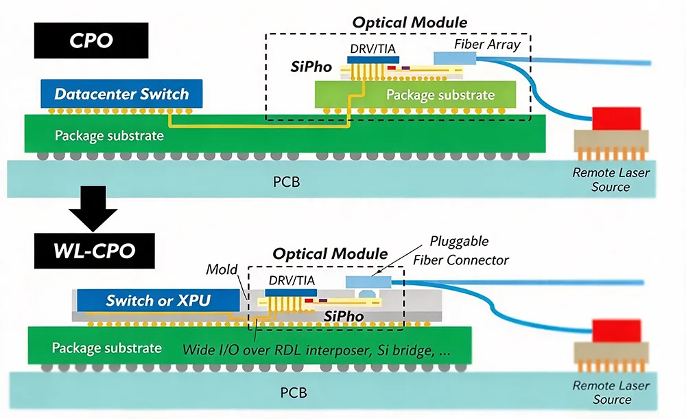
Co-packaged optics (CPO) is built on a simple premise: move the optical engine close enough to the switch ASIC that the electrical channel between them shrinks from centimeters to millimeters. That premise is electrically correct. It is also the source of the PCB’s hardest manufacturing problem in the CPO era.
When the distance is long, the PCB is forgiving. A few micrometers of misalignment, a fraction of a degree of warpage, a slightly different coefficient of thermal expansion (CTE) — these are absorbed by the channel. At millimeter distance, they are not. The CPO PCB stops being a passive carrier and becomes a mechanical and thermal constraint that determines whether the optical link works at all.
This article examines the specific manufacturing limits that the millimeter interconnect imposes on co-packaged optics PCB design and fabrication, and why the challenge is not simply “a shorter trace.”
2. Alignment: From Electrical Tolerance to Optical Tolerance2.1 The Tolerance Collapse
In a pluggable optical module, the electrical interface is a connector. Its alignment tolerance is measured in tens of micrometers, and the optical coupling happens inside the module, isolated from the PCB. CPO eliminates that isolation. The silicon photonics engine sits on or adjacent to the ASIC package, and the optical path must be aligned to the photonic integrated circuit (PIC) at the board or package level.
The numbers are unforgiving. Conventional edge-coupled or grating-coupled approaches require 0.1–1 µm alignment tolerance for acceptable coupling loss. A fiber-to-waveguide alignment must be held within ±0.5 µm to prevent signal loss, a precision that borders on the nanometer scale in practice. Achieving this in a laboratory is difficult. Achieving it across a production panel, on a PCB that has been through lamination and reflow, is a different order of problem.
2.2 Why Passive Alignment Changes the PCB Requirement
A promising path is passive alignment — using etched features or alignment markers on the board to position the optical interface without active feedback. This is cost-effective but less precise than active alignment. A detachable fiber-to-chip coupling platform has demonstrated assembly tolerances of >±30 µm with coupling loss
That tolerance relaxation is significant, but it does not eliminate the PCB constraint. A ±30 µm assembly tolerance still requires the PCB to hold its dimensional stability through lamination, reflow, and thermal cycling. The alignment feature is only as reliable as the board it is etched into. This is where the CPO alignment tolerance conversation moves from optics to PCB process control — and where fabrication capability in a region like Shenzhen, with dense high-layer-count and HDI production, becomes a practical differentiator for CPO programs.
3. Material and CTE: The Millimeter Leaves No Room for Mismatch3.1 The CTE Problem Intensifies
Every CPO assembly combines materials with different thermal expansion: silicon (≈2.6 ppm/°C), the organic PCB substrate (14–18 ppm/°C in-plane, but 40–70 ppm/°C Z-axis before Tg), and the solder or adhesive interfaces between them. Over a millimeter gap, this mismatch is managed by compliance. Over a millimeter-scale interconnect, it becomes a direct threat to optical alignment and electrical continuity.
The photonic chip and the electronic chip may use different material systems — silicon, InP, SiN — with CTEs that are not easily co-packaged with traditional electronic materials. This can cause bonding issues or optical loss at interfaces, and the standard recommendation is to choose thermally compatible materials or add mechanical buffers. At the CPO interconnect scale, a mechanical buffer consumes space that the architecture does not have.
3.2 The Glass Substrate Question
One response to the CTE problem is the use of glass substrates. Glass CTE can be controlled in the 3–5 ppm/°C range, drastically reducing thermal mismatch with silicon wafers, and glass carriers have been reported to deliver 50% less warpage and 35% better positional accuracy than organic core substrates, enabling sub-2 µm redistribution-layer routing on large panels.
Glass is not a drop-in PCB material, and its manufacturing ecosystem is still maturing. But it illustrates the direction of the solution: when the interconnect distance shrinks to millimeters, the substrate’s CTE and warpage behavior become first-order RF and optical performance parameters, not second-order mechanical details.
4. Warpage and Thermal: The Short Path Concentrates Every Error4.1 Warpage Shifts the Optical Axis
On a long electrical channel, board warpage changes impedance slightly. On a millimeter optical interconnect, warpage changes the angle and position of the optical axis. A board that bows by tens of micrometers across the CPO site moves the fiber-to-PIC interface out of tolerance.
This is why low-CTE, low-warpage laminate selection has moved from a “nice to have” to a CPO design requirement. Materials such as Rogers RO1200 (Dk 3.05, Df 0.0017 at 10 GHz, low CTE, supporting mSAP and multiple lead-free reflows) and Megtron 9 (Dk 2.9, Df 0.0005 at 28 GHz, Z-axis CTE below 2.8%) are positioned specifically for CPO host boards and 224G+ interconnect, where every 0.1 dB of channel loss and every micrometer of dimensional drift matters.
4.2 Thermal Coupling at the Hottest Point
CPO places the optical engine near the ASIC — the hottest component on the board. The thermal management problem is therefore not isolated to the ASIC; the optical engine and its alignment features are exposed to the ASIC’s thermal field. Photonic devices are highly sensitive to temperature: even slight variations can shift operating wavelengths or reduce performance efficiency, and without effective thermal design, temperature-induced drift can misalign optical signals and degrade signal quality.
The PCB must therefore provide a thermal path that is both effective and mechanically stable. Thermal vias, copper planes, and low-CTE dielectrics are not independent choices; they interact at the millimeter interconnect site, where heat, expansion, and optical alignment converge.
5. Manufacturing and Test: The Non-Reworkable Constraint5.1 Yield Before Assembly
One of the structural differences between CPO and pluggable optics is reworkability. In CPO, once the heterogeneous integration or assembly process is finalized, the module is virtually non-reworkable. A failed silicon photonics engine cannot be replaced without scrapping the assembly.
This shifts the yield burden upstream. The PCB must be verified before the optical engine is attached. The concept of known-good-die (KGD) verification becomes known-good-substrate verification: the CPO PCB must demonstrate its dimensional accuracy, impedance, and thermal performance before it enters an assembly process that offers no second chance.
5.2 The Assembly Tolerance Chain
The millimeter interconnect is the product of a tolerance chain: PCB fabrication tolerance, die placement accuracy, fiber attach tolerance, and underfill or adhesive cure shrinkage. At each step, the error must remain compatible with the final ±0.5 µm or ±30 µm budget, depending on the coupling approach. The PCB is the foundation of this chain. If the board’s registration or flatness drifts, no downstream assembly step can recover the loss.
6. Short Link, Narrow Window
The promise of CPO is electrical: by shortening the link between the optical engine and the ASIC to millimeters, it removes most of the loss, equalization burden, and power consumption of a long PCB trace. But the electrical gain carries a manufacturing cost. The millimeter interconnect exposes the PCB’s tolerance, CTE, warpage, and thermal stability as parameters that directly affect optical performance, and it removes the buffer that the longer channel once provided.
For programs working with co-packaged optics PCB, the engineering focus should shift from “the shortest possible trace” to “a substrate that is stable at the millimeter scale.” That means:
• Selecting low-Df, low-CTE, low-warpage laminates and validating them at the CPO site, not only in the datasheet.
• Qualifying alignment features on the actual stack-up, in the actual assembly process — whether that process uses sub-micron active alignment or ±30 µm passive coupling.
• Characterizing warpage and thermal drift before the optical engine is attached, because the assembly is not reworkable.
• Treating the PCB as part of the optical alignment chain, not just as a mechanical carrier for the ASIC.
The millimeter interconnect is the defining advantage of CPO architectures. It is also the point where the PCB must become a precision component rather than a support element.
7. Frequently Asked Questions
Q1: Why is the millimeter interconnect harder for the PCB in CPO than a long electrical channel?A: A long channel can tolerate micrometers of misalignment and warpage because the electrical signal has margin. At millimeter distance, the same errors move the optical axis or exceed the coupling tolerance, causing insertion loss that cannot be recovered.
Q2: What alignment tolerance does a CPO PCB need?A: It depends on the coupling approach. Conventional edge or grating coupling requires 0.1–1 µm. Passive alignment platforms can relax to >±30 µm with
Q3: Why does CTE matter more in a CPO PCB?A: The CTE difference between silicon (≈2.6 ppm/°C) and the organic PCB substrate (40–70 ppm/°C Z-axis) turns thermal expansion directly into alignment error and bond stress at millimeter interconnect distances.
Q4: Can glass substrates solve the CPO CTE problem?A: Glass substrates can achieve CTE in the 3–5 ppm/°C range and reduce warpage by roughly 50% compared with organic cores on large panels. However, the glass ecosystem is still maturing, and glass is not a drop-in replacement for every CPO design.
Q5: Why must a CPO PCB be verified before assembly?A: CPO modules are essentially non-reworkable after heterogeneous integration. Once the silicon photonics engine is attached, a PCB defect cannot be fixed by replacing a component. The substrate must be verified for dimensional, impedance, and thermal performance before assembly.
Q6: Which PCB materials are suitable for CPO host boards?A: Low-Df, low-CTE materials such as Rogers RO1200 (Df 0.0017 at 10 GHz) and Panasonic Megtron 9 (Df 0.0005 at 28 GHz, Z-axis CTE below 2.8%) are positioned for CPO host boards and 224G+ interconnect.
Q7: How does thermal management in CPO affect PCB design?A: The optical engine sits near the ASIC, the hottest component on the board. Photonic devices are temperature-sensitive, and thermal drift misaligns optical signals. The PCB must provide an effective thermal path while maintaining mechanical stability at the millimeter interconnect site.
Q8: Does CPO eliminate the need for high-speed PCB traces?A: It reduces the number and layer count of high-speed electrical channels on I/O-intensive switch boards, but it does not eliminate the PCB. The PCB takes on new roles: hosting the optical engine, managing thermal coupling, and providing the mechanical and dimensional reference at the millimeter scale.
Q9: Does passive alignment mean PCB tolerance no longer matters?A: No. Passive alignment relaxes assembly tolerance but shifts the burden onto the PCB’s dimensional stability and alignment-feature accuracy. Board-level warpage or registration drift can still defeat passive alignment.
Q10: What capabilities should a PCB manufacturer offer for CPO programs?A: Low-CTE/low-Df material processing, controlled warpage and registration, mSAP or fine-line capability, and test methods that verify the CPO site dimensionally and thermally before the optical engine is attached.
8. About Us
Richfulljoy supports AI and data-center interconnect programs with high-density, high-speed PCB manufacturing — including low-Df/low-CTE laminate processing, fine-line mSAP capability, and controlled warpage and registration for CPO host boards and silicon photonics engine carriers.
Media Contact
Company Name: Shenzhen Rich Full Joy Electronics Co., Ltd.
Contact Person: Media Relations
Email: Send Email
Country: China
Website: https://www.richpcba.com/


